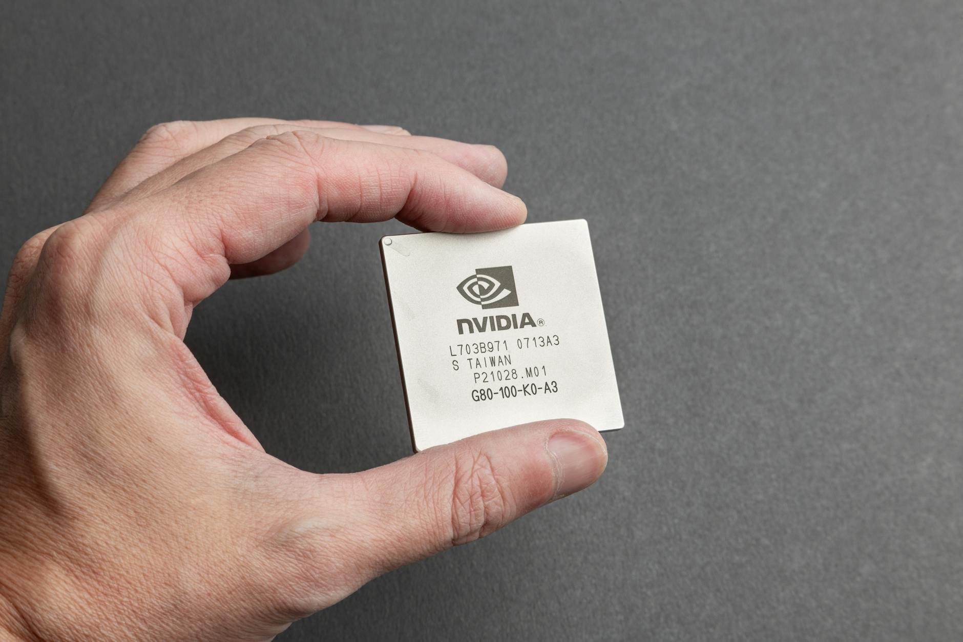
Nvidia Announces $12B Semiconductor Fab Investment in Arizona, Targeting 2027 Production Start
The semiconductor industry’s supply chain map is being redrawn with permanent ink. Nvidia has committed $12 billion to construct a state-of-the-art fabrication facility in Arizona, marking one of the largest single investments in domestic chip manufacturing capacity announced since the CHIPS Act became law. With production scheduled to begin in 2027 and more than 8,000 jobs projected, this represents a fundamental shift in how America’s AI infrastructure will be built.
Strategic Pivot to Vertical Integration
Nvidia’s announcement represents a significant departure from its historically fabless business model. For decades, the company has relied on partners like TSMC and Samsung to manufacture its chips while focusing internal resources on design and architecture. This $12 billion Arizona fab signals a strategic recalibration driven by recent supply chain disruptions and explosive growth in AI chip demand.
The facility will focus on advanced node semiconductor fabrication, specifically targeting production requirements for Nvidia’s next-generation AI accelerators and data center GPUs. This vertical integration move gives Nvidia direct control over a critical portion of its supply chain, reducing dependency on overseas manufacturing capacity during a period when demand for AI chips consistently outstrips available production slots.
Economic Impact and Workforce Development

The 8,000-plus positions created by this investment span the full spectrum of semiconductor manufacturing roles, from process engineers and cleanroom technicians to supply chain managers and quality assurance specialists. Arizona’s existing semiconductor ecosystem—anchored by Intel’s long-standing presence and TSMC’s $40 billion expansion—provides a talent pipeline and supporting infrastructure that makes the state increasingly attractive for major fab investments.
Beyond direct employment, semiconductor fabrication facilities generate substantial multiplier effects. Industry analysis typically estimates that each direct fab job supports three to four additional positions in the regional economy through suppliers, service providers, and consumer spending. For Arizona, this translates to a potential economic impact exceeding 30,000 total jobs when accounting for indirect and induced employment.
The state’s universities have already begun expanding semiconductor engineering programs in anticipation of industry demand. Arizona State University and the University of Arizona have committed to doubling their semiconductor-related graduate program capacity by 2026, creating a sustainable talent development pathway aligned with the 2027 production timeline.
Supply Chain Sovereignty and National Security
Nvidia’s Arizona fab investment directly addresses growing concerns about semiconductor supply chain vulnerability. The concentration of advanced chip manufacturing in Taiwan and South Korea has created geopolitical risk that both industry leaders and policymakers have identified as a critical national security issue.
The CHIPS and Science Act allocated $52 billion specifically to incentivize domestic semiconductor production, and Nvidia’s commitment demonstrates the policy’s effectiveness in attracting major capital investments. While the company has not disclosed the specific federal funding it will receive, projects of this scale typically qualify for substantial manufacturing tax credits and direct grants under the program’s provisions.
This facility will produce chips that power AI training clusters, autonomous vehicle systems, and advanced data center infrastructure—technologies that government agencies and defense contractors have increasingly flagged as requiring secure, domestic supply chains. The 2027 production start date aligns with projected timelines for next-generation AI infrastructure deployments across both commercial and government sectors.
Technical Capabilities and Market Positioning
The Arizona fab will incorporate extreme ultraviolet (EUV) lithography equipment and advanced packaging capabilities, positioning it to manufacture chips at the 5-nanometer node and below. This technical specification is critical—it means the facility can produce Nvidia’s most advanced AI accelerators rather than serving as a secondary site for mature node products.
Nvidia’s AI chip manufacturing strategy has faced capacity constraints as demand from hyperscale cloud providers, enterprise customers, and research institutions has surged. The company’s H100 and upcoming B100 GPU accelerators have experienced lead times stretching beyond six months, creating bottlenecks for customers building large-scale AI training infrastructure.
By bringing advanced fabrication in-house, Nvidia gains flexibility to prioritize production runs, optimize process flows for its specific architectures, and reduce the time from design completion to volume manufacturing. This operational control becomes increasingly valuable as AI chip product cycles accelerate and customization demands from major customers intensify.
Timeline and Implementation Challenges
The 2027 production start date sets an aggressive but achievable timeline. Semiconductor fab construction typically requires three to four years from groundbreaking to initial production, and Nvidia’s schedule assumes site preparation begins in early 2025. The company will need to navigate complex permitting processes, secure water rights in Arizona’s constrained supply environment, and coordinate construction of supporting infrastructure including power substations and chemical delivery systems.
Equipment procurement represents another critical path item. Lead times for advanced lithography tools and deposition equipment currently extend 18 to 24 months, requiring Nvidia to finalize technical specifications and place orders well before facility construction completes.
Reshaping the Semiconductor Landscape
Nvidia’s $12 billion commitment to Arizona semiconductor fabrication represents more than a single company’s expansion—it validates the reshoring strategy that has dominated industry policy discussions for the past three years. Combined with Intel’s Ohio megafab, TSMC’s Arizona expansion, and Samsung’s Texas facility, the United States is rebuilding advanced chip manufacturing capacity at a scale not seen since the 1990s.
For semiconductor industry professionals, supply chain analysts, and investors, this announcement provides a concrete data point for modeling future capacity distribution and regional manufacturing clusters. The 2027 timeline and 8,000-job commitment offer measurable benchmarks against which to track execution and assess the broader success of domestic semiconductor manufacturing policy.
The AI chip demand driving this investment shows no signs of moderating, and Nvidia’s decision to secure its own production capacity through vertical integration may set a template for other fabless chip designers facing similar supply constraints. Arizona’s emergence as a semiconductor manufacturing hub is no longer a projection—it’s infrastructure under construction with delivery dates on the calendar.
Send free SMS worldwide
Reach any mobile number in 200+ countries from your browser. No signup, no app.
Send a free SMS →